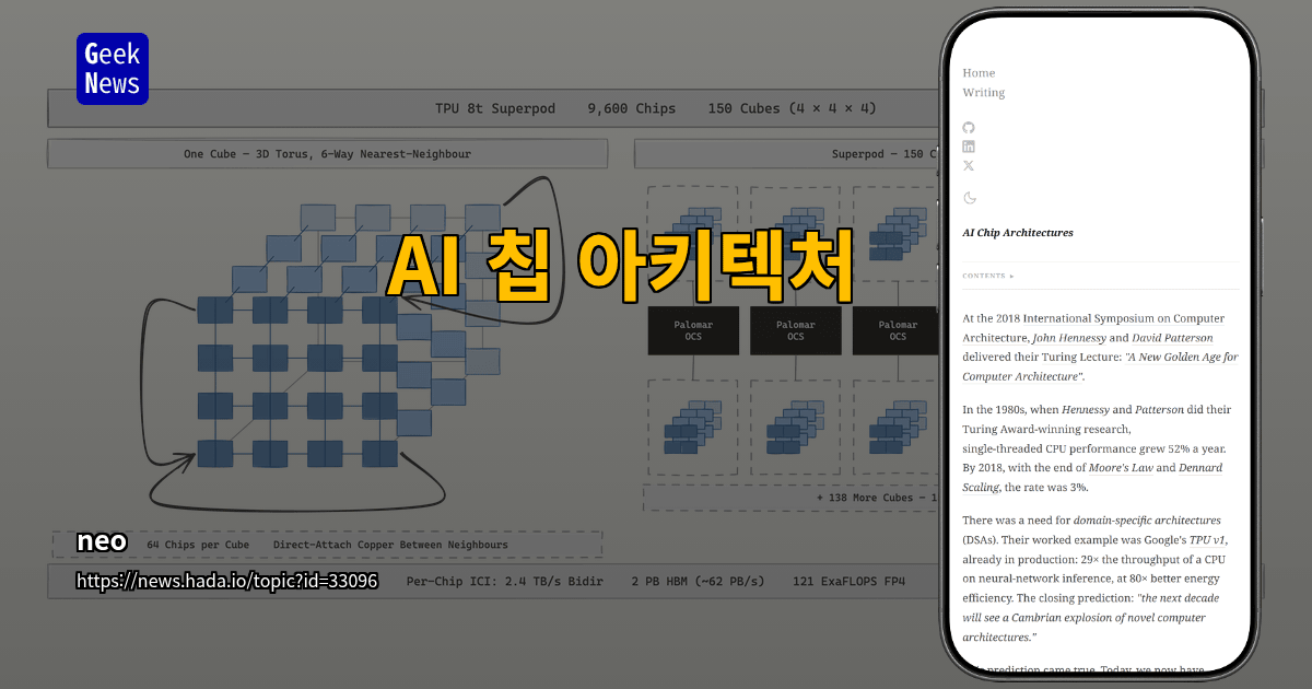
Key Takeaways
- Single-thread CPU performance grew at 52% per year in the 1980s, but that rate had dropped to just 3% by 2018, making general-purpose CPUs structurally inadequate for AI compute demand
- AI compute became the center of the Domain-Specific Architecture (DSA) race, with NVIDIA GPU, Google TPU, AMD Instinct, Cerebras WSE, AWS Trainium, and Groq LPU each entering the market with their own design philosophy
- Each chip adopts a different data-movement strategy, so FLOPs alone cannot determine real-world workload efficiency
Analysis
AI chip architectures have long since stopped converging on a single answer. Single-thread CPU performance climbed 52% every year through the 1980s, but by 2018 that growth rate had collapsed to 3%. Once the era of free lunches from Moore’s Law ended, AI compute demand began demanding its own design language to fill the gap.
The most meaningful point at this stage, in the author’s view, is that “how data moves,” not “how a chip is built,” has become the central axis of AI chip architecture competition. Two chips may quote identical FLOPs yet deliver very different real-world workload efficiency. That gap is each vendor’s design philosophy in action.
Why AI Chip Architectures Diverged
The performance growth rate that fell to 3% in 2018 does not apply cleanly to the large-scale matrix operations behind transformer training. NVIDIA opened the market first with GPU-based AI chip architecture, while Google shipped TPUs designed around its own workloads. With AMD Instinct, Cerebras WSE, AWS Trainium, and Groq LPU all joining in, the Domain-Specific Architecture (DSA) race truly began.
Cerebras WSE chose an extreme approach, treating an entire wafer as a single die. Groq LPU fixes data flow at compile time to sidestep memory bandwidth bottlenecks. AWS Trainium targets price-to-performance, while Google TPU pairs tensor cores with high-bandwidth memory (HBM) to accelerate matrix math. All grouped under AI chip architecture, the operating principles differ sharply.
Data Movement Decides Real AI Chip Architecture Efficiency
What stands out to practitioners is that FLOPs spec sheets do not translate directly into workload performance. Memory hierarchy and interconnect design decide how much efficiency you get for the same compute. NVIDIA GPUs combined HBM with NVLink and NVSwitch to handle bandwidth and scalability at once, while TPUs focused on data-center-scale expansion through pod-level topology.
Groq LPU’s defining difference is not where data lives but when it moves. It uses deterministic execution to remove memory latency variance. Cerebras WSE maximized on-die SRAM to cut external memory round-trips altogether. Even within the same AI chip architecture category, the answer to data movement has split.
How the Transformer Training Stage Shapes the Equation
Training and the prefill stage of a transformer carry a heavy matrix-matrix multiplication share. That stage leans more on compute throughput than memory bandwidth. Chips like the H100, MI300, and TPU v5p paired tensor cores with HBM to push throughput higher. According to GeekNews’s AI chip architecture topic, this layout has become the central axis of the domain-specific silicon race.
By contrast, the decode stage, where token-by-token generation repeats, runs into a memory bandwidth bottleneck. The same AI chip architecture struggles to cover both ends well, so in practice it has become common to mix and match chips based on workload ratios. As explored in a16z’s full-stack AI value chain strategy, chip selection has shifted from simple spec comparison to per-workload decision-making.
Where the Debate Stands
AI chip architecture competition converges into three streams. First, GPUs leverage generality and ecosystem dominance. Second, TPUs and Trainium pursue cost efficiency through in-house workload optimization. Third, Cerebras and Groq LPU offer alternative paths that avoid memory bottlenecks. Which one wins depends on the workload.
Metrics You Must Check When Selecting an AI Chip Architecture
The 52% to 3% collapse in single-thread CPU performance growth is not just a retrospective figure but the starting point for today’s decisions. Comparing chips on FLOPs alone falls into the same trap. Memory bandwidth (GB/s), HBM capacity, interconnect topology (NVLink, ICI, Ethernet), and per-stage workload throughput must all be considered together to surface real efficiency.
A common mistake observed in the field is picking a chip solely because its benchmark score looks strong. In real training and inference pipelines, data preprocessing and communication overhead can eat up 30–50% of total time. That share has to be weighed against the AI chip architecture’s memory hierarchy.
What to Do Right Now
- Profile the stage-by-stage time ratio of your current training and inference pipeline (preprocessing, training, communication, decode).
- Tabulate the target chip’s HBM capacity and memory bandwidth in GB/s and match it to your batch size.
- For workloads with a high decode share, evaluate LPUs; for training- and prefill-heavy workloads, review mixed GPU/TPU deployment scenarios.
- Simulate whether interconnect topology (NVLink, ICI, Ethernet) becomes a bottleneck during multi-node scaling.
- Track each chip vendor’s release notes quarterly and log improvements in memory hierarchy and data-movement design.
Frequently Asked Questions
What is the most important metric in AI chip architecture?
FLOPs alone is not enough. Memory bandwidth, HBM capacity, interconnect topology, and per-stage workload time ratios must all be examined together to surface real efficiency.
How is Groq LPU different from a GPU?
Groq LPU uses deterministic execution to remove memory latency variance. It cuts external memory round-trips, giving it a clear edge in token-by-token decode-stage generation.
Should I choose TPU or Trainium?
If your in-house workload stays within Google Cloud, TPU has the edge. If you are tied to the AWS environment and prioritize price-to-performance, Trainium is a candidate. Both are domain-specific chips, but their ecosystem dependencies differ.
What kind of environment is Cerebras WSE suited for?
It is worth considering when a single model must handle parameter sizes that exceed HBM limits. For typical training and inference pipelines, securing a cost-effective ROI is difficult.
Expert Commentary (AI)
AI Semiconductor Architect
Data-movement-centric domain-specific design is a technically settled direction, but the real contest will be decided by the software stack and economics
The shift to Domain-Specific Architecture (DSA) after the end of Dennard scaling and the slowdown of Moore’s Law is a settled direction the computer architecture community long anticipated, and the framing that “data movement dominates energy and latency over compute itself” is architecturally sound. Groq LPU’s static-scheduling-based deterministic execution, despite its constraints on model size and flexibility due to on-chip SRAM dependence, has proven real differentiation in low-latency inference. Cerebras’s wafer-scale approach, even with yield and cost challenges, presents a unique solution that bypasses the memory wall. That said, the real battleground in this competition is not only hardware indicators like HBM capacity or interconnect topology but also compiler maturity, kernel coverage, and the completeness of the CUDA-alternative ecosystem. Considering the roadmap leading into chiplets (UCIe), HBM generational upgrades, and optical interconnects, the current architectural fragmentation is closer to a transitional landscape before convergence. The diagnosis that the optimal point differs by workload is correct, but the hidden risk in this picture is that architectural diversity inflates ecosystem fragmentation costs and becomes a barrier to entry for mid-sized and smaller adopters.
ML Infrastructure Engineer
Prefill-decode bottleneck separation and mixed-chip deployment match field experience, but multi-stack operating costs and supply chain variables sit between the ideal and the real
The distinction that prefill is compute-bound and decode is memory-bandwidth-bound aligns directly with established practitioner knowledge spanning continuous batching, PagedAttention, and prefill-decode disaggregated serving, and using workload profiling as the starting point for chip selection is the right approach. However, real-world chip choice is driven first by CUDA kernel compatibility, distributed training framework support, instance availability, and HBM supply conditions rather than by spec sheets alone. Theoretically optimal mixed GPU/TPU/LPU deployment carries significant operational cost from maintaining different toolchains and model formats simultaneously. Groq’s deterministic execution has clear strengths in low-latency serving for smaller models, but its support for large-scale training is limited, so applying the “LPU for decode” correspondence to a real pipeline requires model portability validation up front. The cost efficiency of TPU and Trainium is conditional on each cloud ecosystem, so whether an organization can tolerate vendor lock-in becomes effectively the first decision criterion. Over the next two to three years, benchmark reproducibility and migration tool maturity will determine the success of chip diversification strategies.
Critical Analyst
The biggest beneficiaries of the “FLOPs are meaningless” narrative are challengers who cannot win on peak-spec competition and hyperscalers looking to recoup margin
On the surface, the “data movement is what matters” insight reads as technically neutral, but a closer look reveals that the parties who benefit most from this narrative are challengers who cannot catch up to NVIDIA in peak FLOPs competition, and hyperscalers looking to recapture the margins they have been paying to merchant silicon. The interpretation that TPU and Trainium’s in-house chip expansion is a negotiation card and profit-structure reshuffle against NVIDIA’s pricing power, formed during the H100 supply crunch, rather than a pure architectural superiority claim, is the more natural read. The conclusion that “chips are mixed per workload” can also be read as a direction that inflates total chip consumption, leaving open the possibility that the ultimate beneficiary of the diversification narrative is the chip-selling side as a whole. What truly deserves attention is who is redefining benchmark evaluation criteria and in which direction, and the choice of “which metrics to trust” is itself already on the table of competing interests.
Underlying Scenarios
- Challengers like Groq and Cerebras may have propagated the “FLOPs comparison is a trap” framing into industry discourse. This is a textbook positioning move to shift the battlefield onto axes where they are favored (per-token latency, per-user throughput).
- Google and AWS’s in-house chip expansion likely functioned as substantive negotiation leverage against NVIDIA’s pricing power, characterized by supply shortages and high margins. The fact that the timing of in-house chip announcements and expansion overlaps with the H100 shortage and the AI capex race supports this reading.